Materials Characterisation Techniques
Microscopy and spectroscopy are used for the characterisation of a wide range of materials. The microstructural analysis is performed using microscopy [Optical, Scanning Electron Microscopy (SEM) and Transmission Electron Microscopy (TEM)]. For chemical composition analysis different spectroscopy techniques are generally employed e.g., NMR, Raman, FTIR, XRD, XRF and SEM(EDS).
Why Material Characterisation is important?
Keeping in view the needs of future research and development challenges, efficient and robust characterisation techniques are the need of the modern world. Academic and professional researchers need several characterisation techniques for material analysis to confirm their practical work. The importance of these techniques can be related to bulk properties being related to their microscopic structure. Different kinds of materials with a variety of applications can be characterised by using these techniques. Different inputs interact with the material under investigation and provide outputs. These outputs are then studied using several detectors to comment on the material structure (micro, macro, nano, etc.,). There are two common techniques used for material characterisation study: -
- Spectroscopy
- Microscopy
Spectroscopy
Spectroscopy is a widely used technique in material characterisation studies. It is an interaction of radiation with matter. The investigation/measurement of the resultant spectra (absorption/emission) would provide useful information about the material being tested. Spectroscopy is used for material characterisation, astronomy as well as in medical applications. Some of the spectroscopic techniques are discussed below: -

Scanning Electron Microscopy (Energy Dispersive Spectroscopy)
The scanning electron microscopy technique generates images with a magnification of 500,000 times and it is good up to 1nm correction to appear among solid morphology, the topography of surfaces, and their crystal structures. A beam of electrons intermingles with objects and produces secondary electrons (SE) and disperses in the background electrons (BSE) are taken by detectors.
SEMs consist of a source generating electrons, electrons lenses, a vacuum, and the controlling system as well as many icons that examine the output signals. An electron source produces electrons and also accelerates their energy to a width of 0.1–30 kV. Gun selection depends on the cost, lifetime, and decision.
Thermionic Emitter
These are tungsten wires sources that emit electrons due to resistance heat. Accordingly, they have a short life span (30–100 h) large spring size (30–100μm), very wide power distribution (1–3eV), and very low light (1 105A cm 2sr 1), all leading to very low-resolution imaging. However, on average, cheap, not too hard to use, and very convenient for daily requests.
Field Emitter
Field guns are very bright (1,108 angstrom cm-1), the most closely related source of electrons (frequency less than 1eV), and last longer (1000 years). Field-emission guns are basically of three types: Hot, Cold, and Schottky.
Energy Dispersive X-ray Spectroscopy (EDS)
Energy-dispersive X-ray spectroscopy is an analysis technique, which is usually performed during SEM analysis of a material. The EDS method uses those x-rays which hit the sample when an electron beam is bombarded on it and hence the results show the basic composition of a small volume being analysed on the nano-metric scale.
During SEM analysis, the bombardment of the electron beam into a sample area produces x-ray fluorescence due to the atoms coming in their path. The strength of the x-ray photon is not a factor in the production. The EDS x-ray detector takes into account the number of x-rays produced in terms of their strength. The power of x-ray is part of the chemical element from which x-rays are generated.
We can determine the elements present in the sample under study by determining the strength of the x-rays emitted from the generated electron beam. The method being used is called quality examination as it determines only the different types of elements present in the sample. We can also measure the value of already present elements just by using the level of discovery of these x-rays. Such analysis is named quantitative analysis. If the electron beam is swept to analyse the sample area, then EDS can receive x-ray maps presenting the local variability in the under-observation sample.
The SPECTRAL MM is used for fast milling, so samples can be prepared for X-ray spectroscopy and emission techniques. The SPECTRAL MM allows you to preset the amount of material to be removed very accurately with preset in increments of 10 microns. The vertical movement of the milling head is motorised with digital positioning and display on the touch screen LCD and the robust design of the column guarantees high reproducibility.
X-ray Diffraction
XRD technique is an important and widely used method of differentiating objects. With the latest advances in material science and understanding technology, a variety of innovative building materials are made, which needs the development of already in utilisation microscopy techniques so that we can become able to solve different difficult arising problems.
Principle
When an X-ray is targeted onto a solid substance it gets scattered when it hits the revolving electrons. As a result, waves are emitted in different directions, and surely, they affect each other. This interference can be constructive or destructive. It is to be noticed that diffraction from the orderly placed atoms is constructive.
Application
X-ray diffraction is a great non-destructive characterisation technique having extensive usage inside large fields e.g., the structure of the crystal and its size, category detection, the orientation of crystal structure, lattice boundary determination, separation congestion, residual pressure/weight, phase shift, and coefficient of temperature increase.
X-ray Photoelectron Spectroscopy
X-ray Photoelectron Spectroscopy (XPS) is an important tool for the interpretation of the surface and interface characteristics of a compound. It is an extensively used technique in academic research, research and development, and industrial development. XPS works on the principle of the photoelectric effect. Electrons of an atom absorb energy in the form of photons and get emitted from the surface of a solid depending on the kinetic energy. It considers the binding energy of atoms present in any substance. This technique is highly sensitive to the surface properties of the sample.
Advantages of using XPS
XPS has several advantages over other surface property measurement techniques. Some are enlisted below:
- XPS works for both organic and inorganic compounds making its use versatile.
- Can identify potential surface contaminants thus protecting stainless steel from passivating agents.
- Gives you results in less than half an hour making its use feasible in the busy routine.
- Carried out in a highly vacuumed environment which makes it impossible for the environmental impurities to enter the testing procedure.
Hence, XPS is no doubt an expensive technique, but its outcomes make it attractive to be used for the analysis of important surfaces and substances.
Sample Preparation for Material Characterisation
Sample preparation is an important step in material characterisation study to obtain the desired results from the analysis. The sample needs to be representative, homogeneous, and with an even surface to eliminate factors that can influence the results. Surface grinders are table-top and portable machines that are used for steel or any metal preparation for spectroscopy. Pendulum Grinders are used for iron and steel sample grinding and provides sensitive grinding of samples to 0.01mm accuracy. For the preparation of solid metal samples, Kemet offers manual and automatic sample preparation machines - from the small table-top disc surface grinder to an automatic milling machine. With Kemet Sample Preparation Machines, you feel ready for the analysis.

Atomic Force Microscopy
Atomic Force Microscopy (AFM) is the widely used technique to trace the properties of the surface of a membrane, material, or thin film. AFM is also referred to as scanning force microscopy (SFM). It helps the researchers do topographic images that can be used to create a three-dimensional image of the material's surface. Very small details of the surface i.e., up to fractions of nanometre can be found by this technique within no time. As AFM uses a mechanical probe that touches each part dedicated surface, it then creates a detailed 3D image of that surface. Raster scanning is used for this purpose to record the height of the probe at every point. This mechanical probe data is transmitted to software that creates an actual and real topographic detail of the surface.
AFM Sample Preparation
AFM needs the sample to be perfectly designed and prepared so the analysis can be done smoothly without damaging the probe. Kemet sample preparing machines including surface grinders and automatic milling machines offer quick and reliable service for robust sample preparation.
Why use AFM?
AFM has numerous advantages over other microscopic techniques:
- Easily executes various types of samples with minimum sample preparation
- Has 1000 times more resolution as compared to optical microscopy
- Gives a three-dimensional image that helps the study of the surface effectively
- Can be performed in various environments including air, vacuum, and liquid
- Magnetic forces and mechanical properties of the surfaces can be analysed
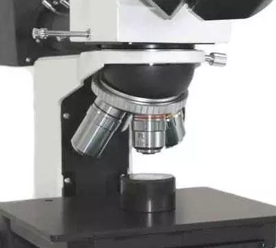
It is one of the most popular techniques that is used in laboratories of schools, colleges, universities, and industries. Visible light is used in this technique with the help of a lens to view the surface of a material. More than one lens is being utilised for extensive surface and interface studies. Simple and compound microscopes are the types of optical microscopy that are commonly used. Imaging the cell structure is also possible by using such techniques. Kemet is offering these kinds of microscopes with exceptional sample preparation methods that can aid your research to an exceptional level. Some are listed below: -
Optical Microscopy
Metallurgical Microscope
This microscope is used to study the highly reflective surface of a metal (the sample must be perfectly polished and flat). To visualise the metal particles or any other kind of particles on a membrane or surface, this microscope can be used.
Stereo Microscope
It is an important type that discovers visual details of samples that cannot be mounted. Therefore, it works with low power and is also referred to as dissecting microscopes. Its speciality is that it works with a huge range of specimens from metals to geological specimens, composites to polymers, plants to insects, etc.
Polarising Microscope
These are used specifically to determine the polarisation characteristics of materials. It works with a polariser lens at the upper and lower side of the specimen.
Digital Microscopes
These microscopes work with built-in cameras, USB, flash drives, and related accessories. These additions can be done to a simple microscope to make them a digital microscope. Wi-Fi connections can also be done for further analysis in live working with samples. Saving data and transferring it to other devices has become much easier with these microscopes.
Material Characterisation Method Examples
Material Characterisation of Concrete
Several techniques are employed to characterise cement and concrete ranging from microscopy (Optical, SEM, TEM), X-Ray spectroscopy, X-ray fluorescence (XRF) and X-ray Diffraction (XRD). The microstructural analysis is conducted to view the internal features of the concrete structure. Rietveld analysis is also conducted to study the structure of concrete. Microscopy is routinely used at cement manufacturing facilities to examine the raw materials, cement clinker etc. Scanning electron microscopy (SEM/EDX) is also used for the microanalysis of crystals or particles of cement. XRF is also used in cement manufacturing to determine the elemental composition of cement/ raw material at different stages of the processing. The use of XRF at different stages of cement production results in a consistent product.
Material Characterisation of Boron Carbide
Concrete is a commonly used construction material in many countries due to its low cost and strength. Due to these advantages, it is also a promising candidate for nuclear reactor applications to protect radiation shielding material. Boron Carbine which is a known neutron absorber material is used as an additive in concrete for shielding applications in nuclear plants. X-ray diffraction, Scanning Electron Microscopy (SEM), Transmission Electron Microscopy (TEM) and Fourier Transform Infrared Spectroscopy (FTIR) are commonly used for the characterisation of boron carbide nanostructure. Sample preparation is done by using polishers, grinders, and cutting-edge technologies.
Material Characterisation of Magnesium Alloys
Magnesium alloys are promising candidates for the aerospace and automotive industry. Material analysis of Magnesium alloys is an important step in determining the requisite structure-property relationship for the intended application. Microstructural analysis of Magnesium alloys can be carried out using Scanning Electron Microscopy (SEM), Transmission Electron Microscopy (TEM) and optical microscopy. This study may be performed on as-cast as well as on hot extruded magnesium alloys. Furthermore, XRD, XRD, and EDS may also be employed based on the scope of characterisation.
Material Characterisation of Casting
Material characterisation of casting is done by using in-situ XRD, ultrasonic testing, SEM, TEM, and energy disruptive spectroscopy. Light microscope is also used to examine the structure of casting.