Precision Lapping and Polishing of Wafers (Gallium Arsenide (GaAs) & Silicon)
Wafer lapping and polishing are vital processes in semiconductor manufacturing, playing a foundational role in achieving the surface flatness, thickness uniformity, and structural integrity required for high-performance devices. As modern technologies increasingly rely on multi-layer lithography and advanced integration techniques, even microscopic variations in wafer topography can cause defocus, misalignment, or process failure. Lapping removes material, corrects bow and warp, and improves overall parallelism, while polishing refines the surface to atomic-level smoothness, eliminating sub-surface damage and achieving precise final thickness. These steps not only prevent defects such as delamination, voids, and adhesion failures, but also enhance device reliability, electrical performance, and manufacturing yield.
The importance of these processes becomes even more pronounced in advanced applications where both geometric precision and flawless surface quality are critical. Photonic devices like GaAs and InP wafers demand ultra-flat, mirror-like surfaces for optimal light propagation and optical clarity. MEMS and sensors rely on strict control of wafer thickness and parallelism for mechanical accuracy and sensitivity. In 3D packaging and wafer bonding, nanometer-scale planarity is essential to form robust, void-free interconnects. Similarly, power electronic devices, including high-voltage GaN and SiC components, require pristine surfaces to prevent premature breakdown and ensure operational stability. In all these areas, the precision achieved through lapping and polishing is not optional—it is fundamental to enabling the next generation of semiconductor innovation.
Lapping and Polishing of Silicon Wafers
Objective: Achieve single-side lapping and chemical mechanical polishing (CMP) of a 4” diameter silicon wafer to a final thickness of 500 µm, with a target surface finish (Ra) of 1–2 nm.
Material and Equipment: The wafer processing task involved a monocrystalline silicon wafer with an initial thickness of approximately 529 µm. The objective was to reduce the thickness to a target value of 500 µm while achieving an ultra-smooth surface finish in the range of Ra 1–2 nanometers. To meet these stringent requirements, two precision finishing processes were employed: an initial lapping stage using a water-based aluminium oxide slurry, followed by chemical mechanical polishing (CMP) with Col-K(X) slurry.
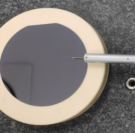
Lapping Process: The lapping operation was performed using a Kemet 15 lapping machine equipped with a Pyrex glass plate and a ceramic conditioning ring. The abrasive medium was aluminium oxide slurry, a water-based solution ptimised for consistent removal rates. The wafer, wax-mounted onto a ceramic block, was processed individually using an applied load comprising a 1 kg ceramic block and an additional 1.8 kg stainless steel (SUS) weight. The plate operated at 15 RPM for a duration of 45 minutes.
The results of this step showed that the incoming wafer thickness ranged from 0.526 mm to 0.529 mm, and was reduced to 0.504 mm to 0.506 mm, yielding a material removal of approximately 0.023 mm. The resulting surface roughness was measured at 0.334 µm, and the material removal rate (MRR) was approximately 0.0005 mm/min. While this process effectively achieved significant material removal and planarization, the surface roughness remained well above the desired nanometer-level specification.
CMP Process: To further refine the wafer surface and achieve the target thickness, chemical mechanical polishing was conducted as the second stage. This process also tilised the Kemet 15 machine, but with a SC1535 polyurethane (PU) polishing pad. The slurry consisted of Col-K(X), enhanced with 100 ml per liter of hydrogen peroxide (H₂O₂) to improve chemical reactivity. The same ceramic conditioning ring was used, and the wafer was wax-mounted as before. However, this time a higher load was applied—1 kg ceramic block plus a 4.1 kg SUS block. The process ran at 15 RPM for 60 minutes.
This polishing step brought the wafer thickness down further, from an incoming 0.504–0.506 mm to an outgoing 0.500–0.502 mm, with a material removal of around 0.004 mm. The resulting surface roughness improved significantly to 0.008 µm (8 nm), and the material removal rate dropped to 0.00006 mm/min. Although the final thickness met the 500 µm target, the achieved surface finish still fell short of the desired 1–2 nm specification.
The combined lapping and polishing process successfully met the dimensional requirement, with the final wafer thickness falling within the 500–502 µm range. However, the surface finish achieved was 8 nm Ra—above the target range of 1–2 nm. Further process ptimisation may be needed to close this gap and meet increasingly stringent surface finish requirements.
Surface Finish (Ra) Achieved 8 nm
Final Material Thickness Achieved 500–502 µm
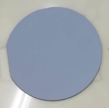
Surface Finishing of Gallium Arsenide (GaAs) Wafers
Gallium Arsenide (GaAs) is a compound semiconductor known for its superior electronic properties, particularly in high-frequency and optoelectronic applications. However, its brittleness and sensitivity to mechanical stress present challenges during wafer preparation. The goal of this test was to process a 2” GaAs wafer to a high optical finish without scratches or residual sub-surface damage, using single-side precision techniques.
Objective: Perform single-side lapping and polishing of a 2” diameter GaAs wafer to achieve a defect-free, mirror-finish surface.
To meet the stringent surface and geometric criteria, the wafer underwent a three-stage surface preparation process. This included an initial lapping stage to remove material and planarize the surface, followed by a first-stage polish to eliminate sub-surface damage from lapping, and finally a second-stage polish for fine surface enhancement and final finishing.
Process Details
Single-Side Lapping: The lapping operation was conducted on a Kemet 15 machine using a flat Pyrex glass plate and aluminium oxide as the abrasive. The wafer was wax-mounted onto a 1.2 kg ceramic block and subjected to an additional 3.5 kg of load. Operating at 30 RPM for 60 minutes, the process effectively removed approximately 0.76 mm of material. The resulting wafer exhibited excellent planarity, with achieved parallelism within 0.002 mm. No processing issues were reported, indicating a stable and efficient material removal phase.
First Polishing Stage: In the first polishing step, the same Kemet 15 system was used, this time fitted with an ASR-H polishing cloth and slurry 1-WHVS2-PC-STR. The load configuration remained the same as in the lapping stage. The plate rotated at 15 RPM for 65 minutes, during which sub-surface damage from lapping was effectively removed. This stage preserved good parallelism, achieving a result of approximately 0.003 mm. It also significantly improved the wafer’s surface quality in preparation for the final polish.
Second Polishing Stage: The final polishing stage was performed using a CHEMO PAD 7 (NC-HS) polishing cloth in combination with a 0.3 µm Alpha Alumina slurry, enhanced by a 20% bleach additive. No additional weight was applied in this stage. The process ran at 15 RPM for a brief 2–3 minute interval, aimed at enhancing the visual quality of the surface. While the wafer likely achieved a mirror-like finish as intended, parallelism decreased slightly to around 0.005 mm.
Final Surface Quality: Upon completion of the three-stage process, the GaAs wafer exhibited a visually flawless, mirror-like finish with no visible scratches or lines, based on visual inspection. Geometrically, the wafer retained high flatness and parallelism throughout most of the procedure, although a minor deterioration was observed following the final polish. Overall, the process proved effective in balancing optical quality and geometric precision, with particularly strong results in the initial lapping and first-stage polishing phases.